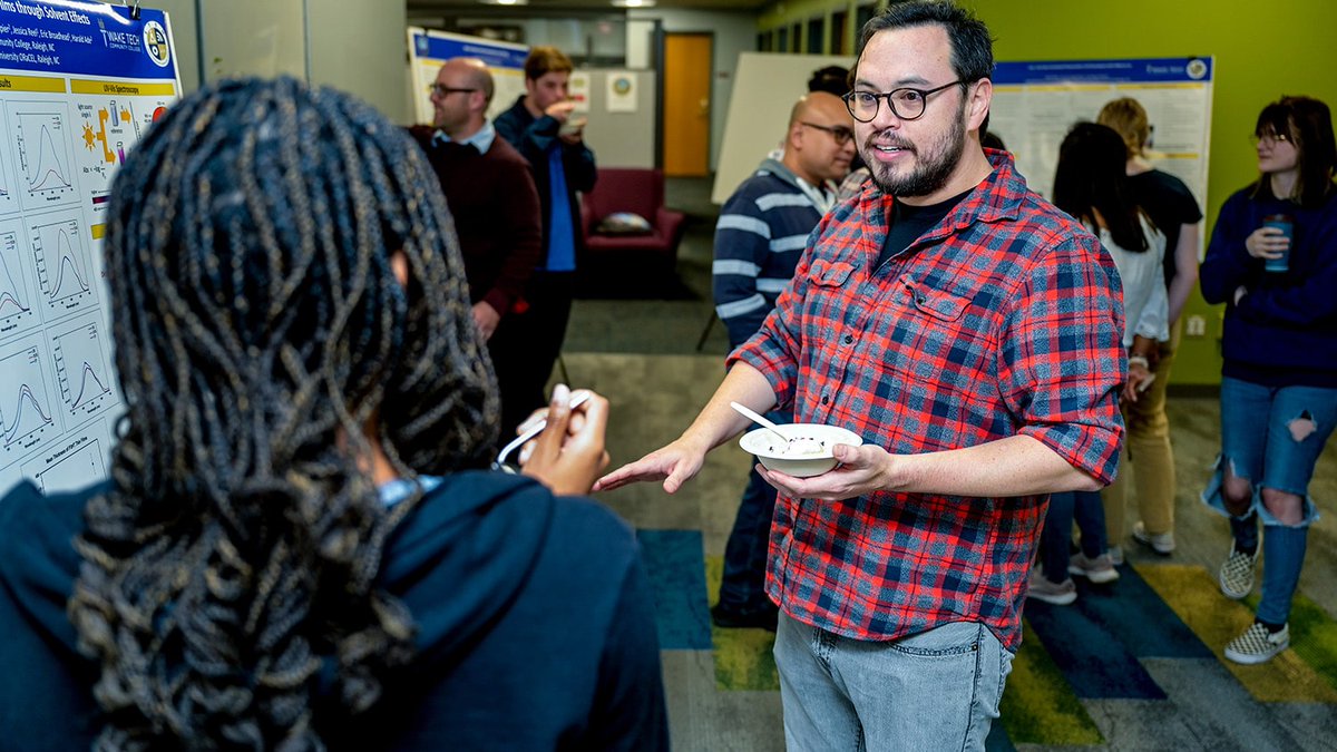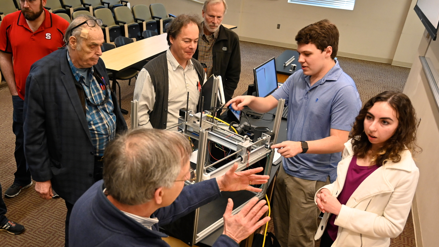
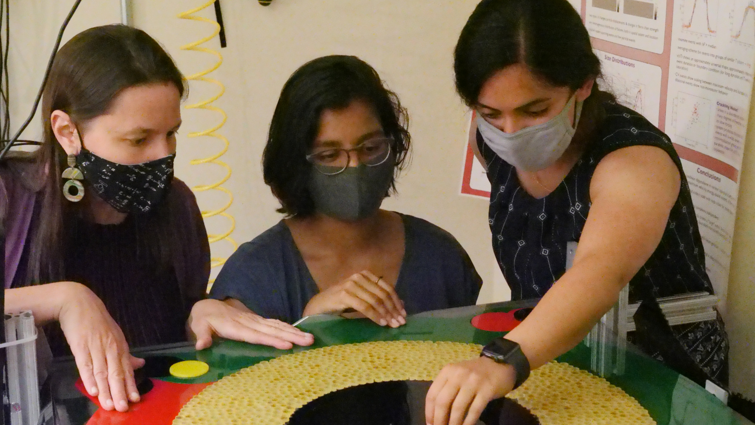
Extraordinary Research
8 AAAS Fellows
Our faculty includes eight fellows of the prestigious American Association for the Advancement of Science.
From NC State graduate student at the lab of @FrohlichCarla to Assistant Professor at Oregon State University (@OregonState)!
Congratulations to alumnus @sanjanacurtis on the next step of her career!!
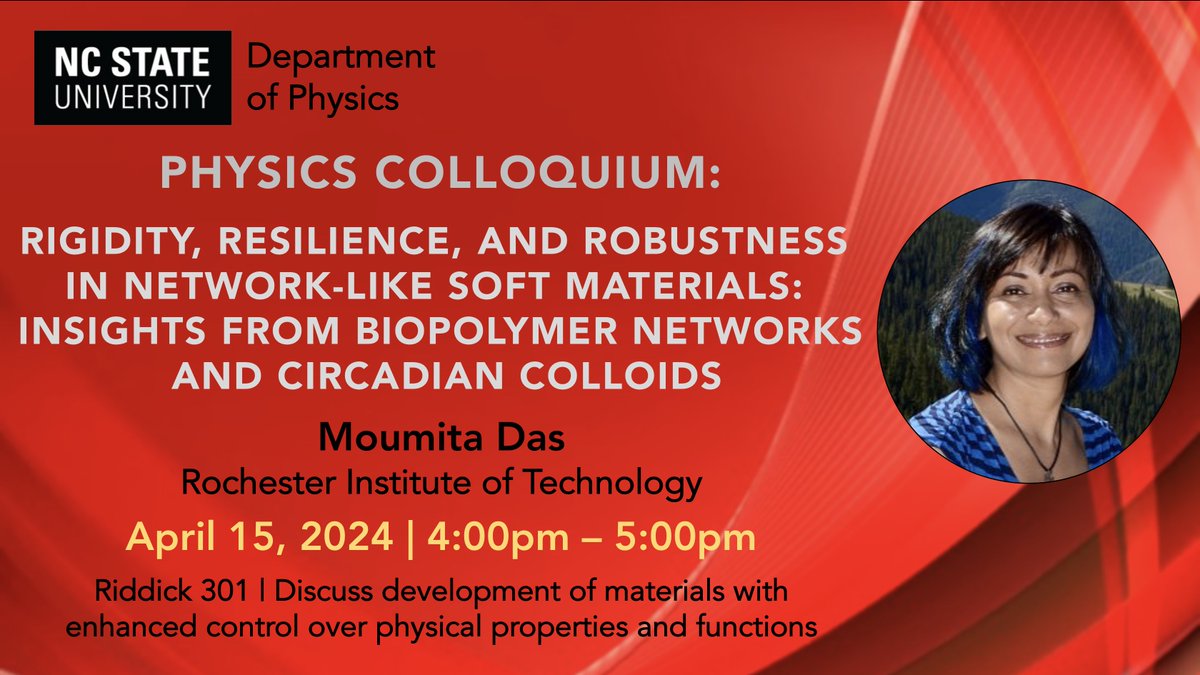
Join us for the colloquium today from 4-5pm in Riddick 301! Dr. Moumita Das from Rochester Institute of Technology will discuss "Rigidity, Resilience and Robustness in Network-like Soft Materials: Insights from Biopolymer Networks and Circadian Colloids".
https://physics.sciences.ncsu.edu/event/physics-colloquium-moumita-das/
.@ncstatephysics graduate student Ben Hines’ journey at NC State goes back 15 years and led to him pursuing a doctorate in physics.
Learn more about his story.
➡️: http://ncst.at/Jwh150R9yFV